Request pricing

Cathodoluminescence fundamentals

Learn everything that you need to know about cathodoluminescence, how it is generated, what it can be used for and how it can be applied in various fields.

Chapter 1

What is cathodoluminescence?

Cathodoluminescence (CL) is light or electromagnetic radiation ranging from the ultraviolet (UV) to the near-infrared (NIR) regime of the electromagnetic spectrum, which is generated by fast electrons (cathode rays) of an electron beam. 

When an electron beam (from a scanning electron microscope for example) interacts with a material, a multitude of processes occur which can be employed for various kinds of microscopy. Besides electron signals, a broad spectrum of electromagnetic radiation is generated through a variety of incoherent and coherent emission processes.


cathodoluminescence-solutions-figure1


https://request.delmic.com/hubfs/Website/Solutions%20Geology/Subsolutions%20page%20Sedimentary%20Rocks/SedimentaryRocks_Featured.jpg

Subscribe to the CL newsletter

Would you like to receive monthly updates on the cathodoluminescence developments and applications? Fill in the form below!

chapter 2

How can you image cathodoluminescence?

Cathodoluminescence is most commonly performed in a scanning electron microscope. In a vacuum chamber containing the sample of interest, an electron beam is focused on the sample.

The light, which is generated, then has to be collected with a collection optic (e.g. mirror or objective), or directly captured by a CL detector in the chamber. When light is collected by an optic, it is directed towards a light detection unit. This detector can then be used to characterize various aspects of the light signal such as its intensity, color, and more.


https://request.delmic.com/hubfs/Website/Webinars%20Thumbnails/2021%20Update%20Webinar%20Thumbnails/2021_CL%20Fundamentals%20Series_ResourceLib_Thumbnail.jpg
Webinar

Introduction to cathodoluminescence

Watch now
chapter 3

Cathodoluminescence and other SEM-based techniques

Various SEM techniques exist that harness signals which occur when a material is excited with an electron beam. The most commonly used techniques, such as secondary electron (SE) and backscattered electron (BSE) detection, electron backscatter diffraction (EBSD) and energy-dispersive x-ray imaging (EDS), can be used to obtain various types of information about the material.

Secondary electrons (SE) detection is a detection of low-energy electrons, with which it is possible to collect secondary electrons only from the top few nanometers of material. This technique is sensitive to surface topography and also shows (minor) material contrast.

Backscattered electrons (BSE) detection is primarily sensitive to density and atomic number and as such can be used to obtain material contrast.

With electron backscattered diffraction (EBSD) the crystal structure and crystal orientation can be studied.

Energy-dispersive X-ray spectroscopy (EDS) probes core transitions in a material and as such can be used for quantitative elemental analysis

Cathodoluminescence can provide unique information, complementary to these techniques. First of all, it allows observing an emission energy range of 0.5 to 6 eV which includes a large variety of important physical processes. Information about the composition, crystal structure, and the electronic band gap can be obtained for example. Furthermore, many trace elements or dopants, can be sensitively detected with CL because they have different optical transitions than the bulk materials they are embedded in. Similarly, it is possible to look at crystal defects as these can alter the local optical properties of the material. With CL you can also image optical resonances and guided modes in a range of (resonant) photonic and plasmonic systems. Combined with other SEM-based techniques, CL can be used to produce a very complete material analysis.  

https://request.delmic.com/hubfs/Social%20Media/CL%20FAQ_Animated%20Banner%20(1).gif
frequently asked questions

Learn more about cathodoluminescence imaging on the FAQ page

Check out questions about CL
chapter 4

What kind of data can you get with cathodoluminescence?

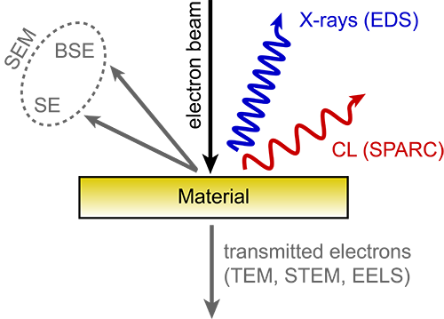
Cathodoluminescence emission can be used to explore many fundamental properties of matter. It can be used to study light transport, scattering, electronic structure of a material, resonant phenomena and much more. It thus presents a valuable source of information for fundamental research as well as applied research with a direct link to industry. Different types of cathodoluminescence detection, also known as imaging modes, can open up new insights and layers of information about your sample. Here are the six most commonly used imaging modes.

Fast-intensity imaging

To obtain cathodoluminescence contrast intensity imaging is commonly performed. A fast photomultiplier tube (PMT) detector is used for large-scale imaging, enabling rapid inspection of large areas, and efficient region-of-interest finding. A filter wheel is present for spectral differentiation.
Applications: This mode is particularly useful for imaging larger areas which is often required in geological applications for example.

Read more in the technical note: Cathodoluminescence intensity mapping.

20200414_SPARC_ImagingModes_FastIntensity

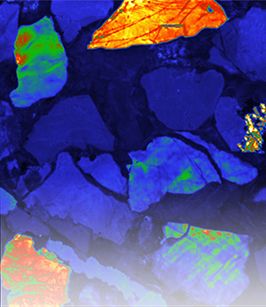
Hyperspectral imaging

Visualizing the wavelength distribution (spectrum) of the material in a parallel manner
Applications: This imaging technique can help you to obtain valuable information on the local optical and structural properties of (nano)materials, such as semiconductors, as well as geological samples.

Read more in the technical note: Hyperspectral cathodoluminescence imaging.

20200414_SPARC_ImagingModes_Hyperspectral

Angle-resolved imaging

Studying how your sample emits and scatters light is possible with angle-resolved cathodoluminescence. Each point of the acquired camera image corresponds to a unique emission angle: this allows characterization of material performance in terms of directivity.
Applications: Angular profiles acquired with this imaging mode are very valuable in the field of nanophotonics.

Read more in the technical note: Angle-resolved cathodoluminescence imaging.

20200414_SPARC_ImagingModes_AngleResolved

Polarimetry and polarization filtered spectroscopy

Measuring the polarization of light reveals in what direction the electro-magnetic fields oscillate. This technique allows measuring the polarization state (Stokes vector) of cathodoluminescence for different emission angles.
Application: This mode can be used for comprehensive measurements of coherence, scattering, and chirality.

Read more in the technical note: Polarization-filtered cathodoluminescence imaging.
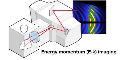
20200414_SPARC_ImagingModes_Polarimetry


Lens-scanning energy-momentum (LSEK) Imaging

This imaging mode allows users to acquire high-resolution datasets resolved both in angle and wavelength, for any given location on the sample. It is a great tool for tracking the directionality through energy and momentum space with very high precision.
Applications: LSEK can be applied to a wide range of dispersive and anisotropic (photonic) systems, paving the way for a broad range of studies in such applications as solid-state lighting, photovoltaics,  and sensing. 

Read more in the technical note: Energy-Momentum cathodoluminescence imaging.

20200414_SPARC_ImagingModes_EnergyMomentum

Time-resolved cathodoluminescence imaging

Time-resolved cathodoluminescence is a technique in which you look at the time dynamics of the cathodoluminescence emission process. Performing time-resolved imaging is possible with the optional Lab Cube time-resolved module or streak camera. The Lab Cube can be used to measure lifetimes as well as the second-order autocorrelation function of the emission, also known as g(2)
Applications: Time-resolved cathodoluminescence imaging is highly relevant for a wide range of applications, including semiconductors for photovoltaics, light-emitting devices, as well as for (single) emitters for quantum information processing and sensing.

Read more in the technical notes: Lifetime cathodoluminescence mapping and Cathodoluminescence g(2) imaging.

20200414_SPARC_ImagingModes_TimeResolved

https://request.delmic.com/hubfs/Social%20Media/SPARC%20Spectral_Integration%20Illustration_Social%20Media.png
SPARC Spectral

Configure your ideal cathodoluminescence system

Try now
chapter 5

How can I apply cathodoluminescence to my research?

Given its sensitivity to a range of fundamental processes in materials, its ease-of-use, and high spatial resolution, cathodoluminescence (CL)  is a highly valuable tool in microscopy for analyzing material properties at very small length scales.

CL is highly relevant to the field of nanophotonics. It is applicable to metallic as well as dielectric and semiconductor nanostructures, including nanoparticles, nanowires, metamolecules, metasurfaces, and photonic crystals. These structures find applications in (bio)sensing, fluorescence enhancement, non-linear optics, low-threshold steam generation, LED’s, solar cells, integrated photonics, lasers and much more.

CL is an ideal tool for studying geological samples and getting additional contrast and spectroscopic information down to the resolution of a scanning electron microscope. The cathodoluminescence emission from a rock gives insights into crystal growth, zonation, cementation, replacement, deformation, provenance, trace elements, and defect structures. This can be used to fingerprint rocks and reveal interesting spatial textures on a submicron scale. Cathodoluminescence is often combined with other analytical tools such as SIMS, LA-ICP-MS, APT, BSE, EBSD, EDS, WDS and μCT for a more complete understanding of all relevant rock properties.

Ceramics, dielectrics, and (compound) semiconductors play an important role in many devices and functional materials, including scintillators, phosphors, high-power electronics light-emitting-diodes, diode lasers, and solar cells amongst others. Nanostructuring is employed increasingly for optimization of the optical properties in such materials. Cathodoluminescence can be used to study these materials (both in bulk and in nanostructured materials) and to determine their light-emitting properties at the nanoscale.

Finally, CL is also increasingly applied to soft matter, including polymers and biological tissues.

https://request.delmic.com/hubfs/CL%20Publications%20list%20Social%20Media2.png
Publications list

Check out our cathodoluminescence publications

View the list
chapter 6

Sample preparation for cathodoluminescence imaging

Generally the following preparation steps can be taken:

  1. Check whether the sample is vacuum compatible. If the surface is dirty it can help to clean it with a chemical clean (e.g. isopropanol, acetone) or reactive ion etching with oxygen, for example.
  2. Check if the sample surface is flat enough. Preferentially large differences (> 0.1 mm) are avoided. 
  3. The sample needs to be conductive enough to prevent charging effects in the SEM. Coating with the sample with a thin layer carbon or metal works well for this purpose. Low vacuum mode imaging which is available in some SEMs can mitigate charging effects.

The most common preparation technique for geological materials is thin sectioning (20 to 30 microns) or resin embedding. Man-made materials, on the other hand, such as semiconductor wafers, are normally flat and conducting already, so no additional preparation is needed in most of the cases. Additionally, next to the abovementioned materials, it is possible to look at the materials in the powder form. For that purpose, the powder can be put on a carbon tape to fixate it and also coat it with carbon or metal if needed.

It is important to note that these steps are generally also needed to prepare the sample for general SEM imaging, so CL imaging does not require any additional work to sample preparation. 

https://request.delmic.com/hubfs/Social%20Media/CL%20FAQ_Animated%20Banner%20(1).gif
frequently asked questions

Learn more about sample preparation on the FAQ page

Check out questions about sample preparation