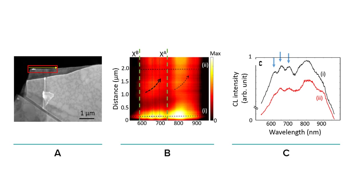
Use the right products to get the right results
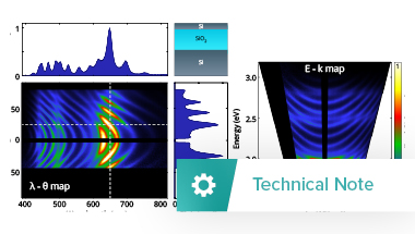
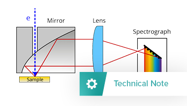
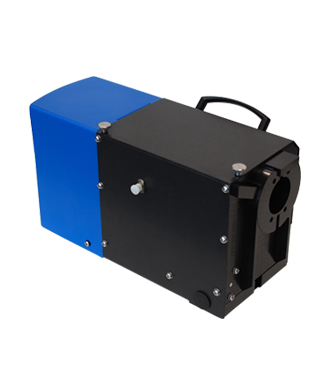
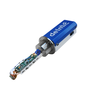
Delmic CL solutions offer a range of powerful and user-friendly cathodoluminescence detectors, which can help you learn more about 2D materials. Choose the product fitting your research!
Don’t know which product is for you?
Get in contact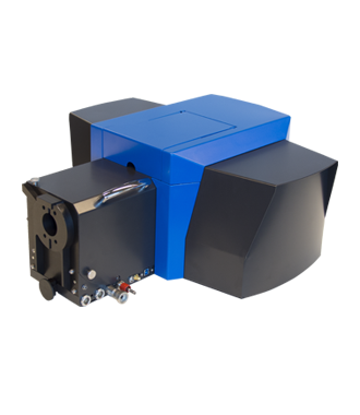
%20imagingRES_380x215.jpg?width=390&name=Image%20Thumbnail%20Technical%20note%20CL%20g(2)%20imagingRES_380x215.jpg)